CMOS Yield Analysis
CMOS IC Yield Analysis
Overview
I had the opportunity to be the Principal Investigator on a phase 2 SBIR Air Force program called AERIA. In this program the goal was to make rectangular shaped Infrared LED (IRLED) emitter hybrids. The hybrids consisted of a CMOS die called a Read-In-Integrated-Circuit (RIIC), and an IRLED emitter die that were bump bonded together. Prior to hybridizing the RIIC and the IRLEDs together the RIIC with the highest pixel operability had to be found. (A more complete write up about the AIREA program can be found in the AIREA project section).
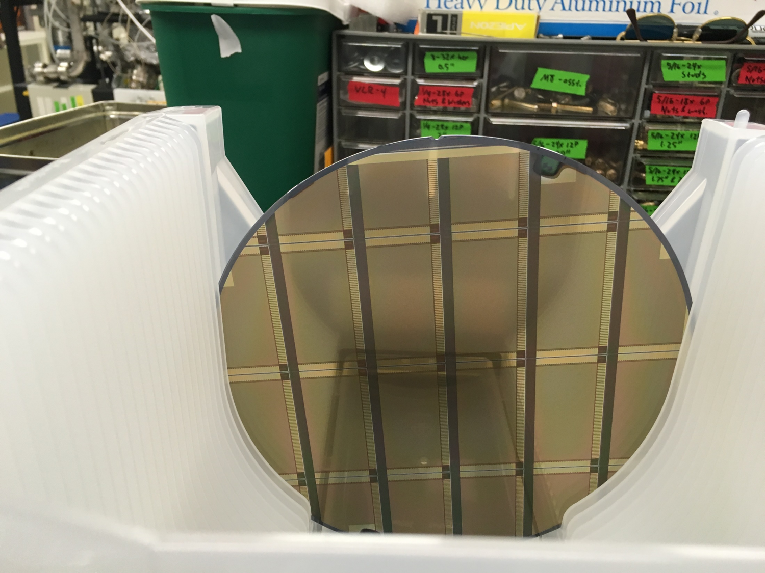
The RIICs are rather large dice. They measure 2 inch x 1 inch, and have a pixel resolution of 2048 x 1024. Which means there are ~2 million pixels in each array. This is not a small task to test all of the RIIC pixels! An 8 inch CMOS wafer with 8 AIREA RIICs on it is shown in the picture below.

These RIICs have bond pads on three sides of them. The bond pads are visible in the image above and are the thick outline visible on the three sides of the rectangles. Four wafers were ordered in total. It was believed that with 32 RIICs there was a high probability of having at least two RIICs with high pixel operability.
Lab Setup
A lab setup was constructed. The setup was constructed in a clean room environment to protect the CMOS wafers from contaminants. The setup included a probe station with a custom probe card that matches the bond pad layout of the AIREA RIICs, two Keithley’s were used to perform the current and voltage measurements. A python class was written for controlling the Keithley’s over RS-232 to automate the testing process (code is available on my github). The data was then stored on a network computer hard drive for later analysis. The lab setup is shown in the picture below.

IC Grading Metrics
RIICs were graded based on several metrics that can be broken into power rail shorting, and pixel current voltage (I-V) curves. The power rail shorting is an easy measurement. A probe card is lowered onto the bond pads this creates and electrical connection with a particular die. A multimeter is then used to check the resistance between the several different voltage rails. If any of the voltage rails are shorted together the die is marked as defective.
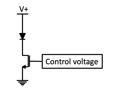
The pixel I-V curve metric requires an understanding of the CMOS circuitry in the RIIC. A simplified view of the circuitry in the RIIC pixel that drives the IRLED attached to the pixel is shown below. A NMOS transistor is shown connected to an LED in the diagram below. The control voltage is an analog voltage that is an input to the RIIC and generated off-chip in what is called the Close Support Electronics (CSE). The control voltage is proportional to the amount of current that will be supplied to the LED. In this way the brightness of the LED can be modulated. Due to fabrication yield issues in CMOS fabrication there are several failure mechanisms in the pixel cell. One is that the NMOS transistor does not work well and cannot supply adequate current to the LED. The second is that the NMOS transistor is non-functional and will produce no LED current. The third is that the control voltage line in the pixel is shorted to a high value and will cause the pixel to be always on. The fourth is that the pixel cannot be addressed because of bad addressing circuitry. It’s important to test each RIIC and choose the ones with the best pixel operability.

Random Sampling
Due to the enormous amount of pixels and the speed at which the Keithley’s operate it would take too much time to test every pixel in the array. A randomly generated map that selects 10% of the pixels was made to decrease the time from several weeks to several hours of testing per RIIC.
Determining What a Good Pixel Is
Good is a subjective word. When looking at plots of I-V curves it is possible to visually inspect and say “good enough.” However, this is not a good method because one it is time consuming and two it is not consistent. A method for determining what a good pixel in the context of our application had to be determined. I decided that the best metric was to make a small CMOS test chip that just had the NMOS transistor. The image below is a zoomed out view of the cadence layout. It’s not possible to see but there are several transistors per test chip.
By measuring the I-V curves of these transistors it was possible to extract the I-V curves of the NMOS transistor used to drive the LED without any of the parasitics or complications of the RIIC. The data collected for all of these transistors was then averaged and combined into one I-V curve. The gate leakage was also measured and averaged during this process. This yielded a “good” curve to compare the operation of the transistors on the RIIC against. A large benefit of having the pure I-V curves of the transistors is that a standard can be set for acceptable limits of gate leakage, and maximum current. This is not limited to the data collected. It was possible to adjust the allowed gate current leakage by adding a constant value to the collected data.
This “good” pixel curve was also compared against the median curve of the RIIC to determine if there was a constant shift in performance up or down of a RIIC.

Data Analysis
Data analysis was conducted in Python with NumPy and SciPy. “Bad” pixels were chosen based on how many standard deviations their measured points were from the corresponding points in the “good” curve. This method proved to particularly effective at determining “bad” pixels.
Results
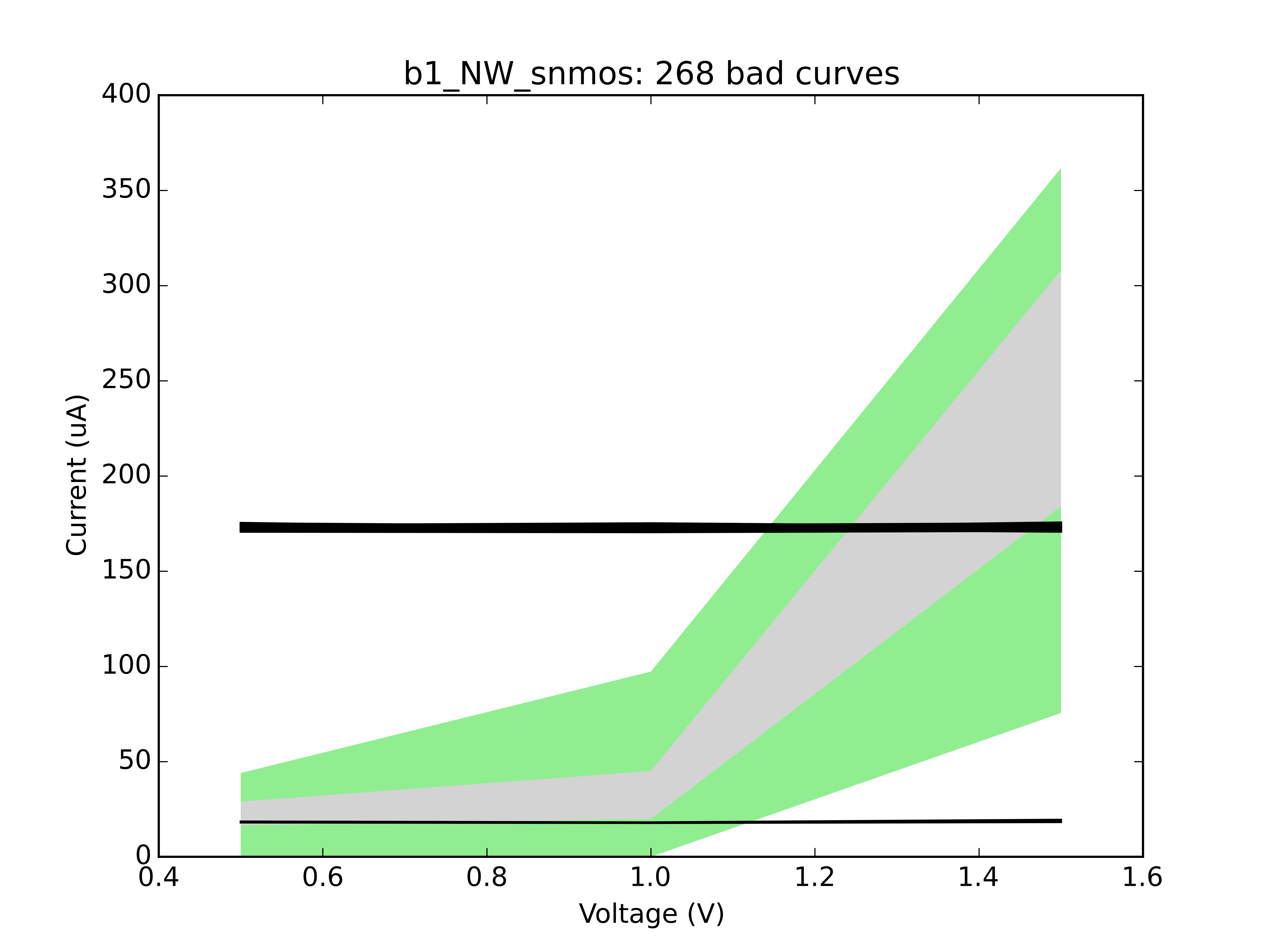
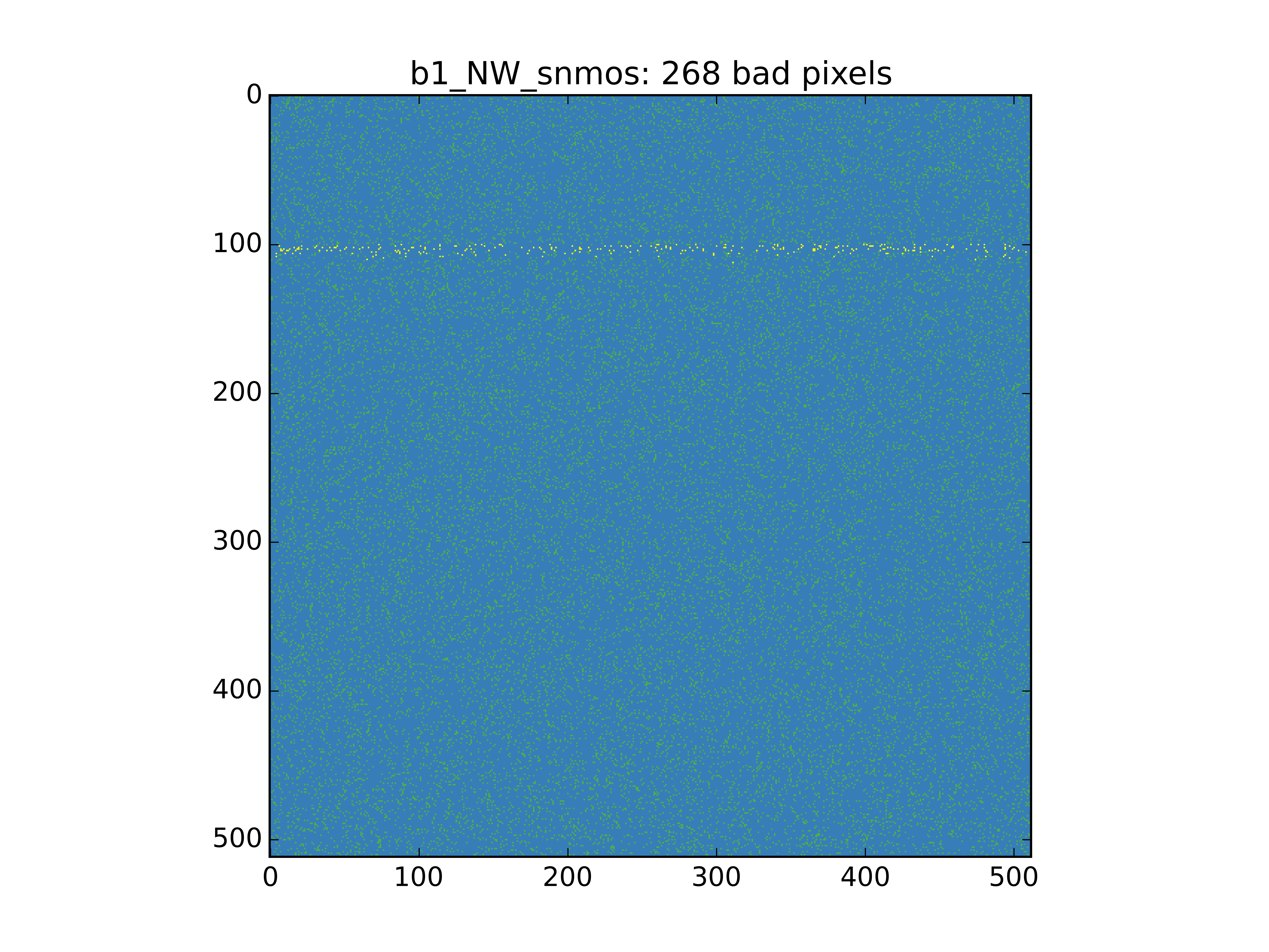
Even with only sampling 10% of the pixels there are still ~200,000 pixels. This is too many pixels to plot every I-V curve. I developed a plot that is shown below. The grey area represents 80% of the curves, while the green area shows the outliers. Pixels that are chosen as bad are shown in black. In the second image the location of the pixels that were chosen as bad are shown. This is useful because randomly distributed dead pixels may be able to be fixed algorithmically, but a dead column or row will not be able to be averaged out.


